Buried core multi-layer printed circuit board, core embedded technology and multi-layer blind buried hole design of the organic combination.
1, features and features
Integrated copper thickness ≥ 400μm thick copper and multi-layer circuit design in one, to meet the high current through electronic products, but also to achieve high-density placement needs in the automotive electronics, high power power modules and other fields widely used.
2, technical background
With the rapid development of automotive electronics and power communication modules, it is possible to integrate power supply, provide high current and high reliability. The thick copper foil printed circuit board has become a popular product of PCB industry.
At the same time accompanied by the development trend of high-density electronic technology, the traditional 4-6OZ conventional thick copper has been difficult to meet its performance requirements, 10-12oz and more ultra-thick copper multilayer demand is increasing, especially in high power Rectifier equipment needs obvious.
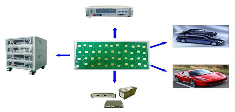
3, the application areas
4, the core technology
Positive and negative step-by-step deep etching technology: an effective solution to the problem of thick copper wire etching difficult;
Positive and negative line alignment precision control technology: effectively enhance the accuracy of the two graphics coincidence;
Ultra-thick copper by laminating technology: the effective realization of the ultra-thick copper multi-layer printed circuit board production and processing.
5, patented technology
12oz ultra thick copper multi-layer printed circuit board processing method (invention patent)
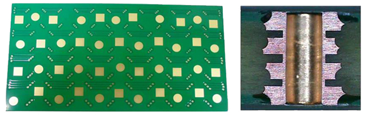
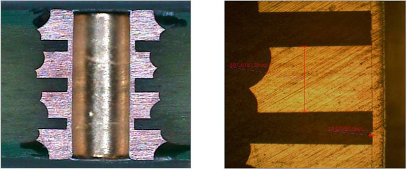
6, ultra-thick copper drilling quality
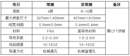
7, thick copper processing capacity
 >HOME >Technology
>Application of security
>PCB
>HOME >Technology
>Application of security
>PCB